Most Commented
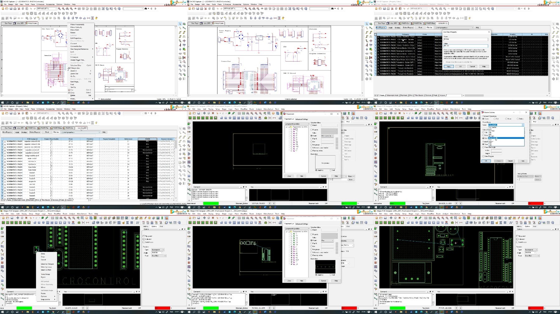
Udemy - PCB Design in Cadence OrCADAllegro Basics to Expert level


Description material

7.02 GB | 00:28:10 | mp4 | 1920X1080 | 16:9
Genre:eLearning |Language:English
Files Included :
001 Course Promotional Video (15.29 MB)
002 Things We Learn Here (21.91 MB)
001 How to do Registration and Log in (21.02 MB)
002 How to Download the PCB Design (Free Trail) Tool (27.54 MB)
003 An Installation Guide (11.6 MB)
001 What are Printed Circuit Boards (33.03 MB)
002 Types of Printed Circuit Boards (23.08 MB)
003 Classes of Printed Circuit Boards (28.6 MB)
004 Levels of Printed Circuit Boards (23.39 MB)
005 What are components of PCB (17.93 MB)
006 Do you know about Thickness (19.17 MB)
007 Lets Discuss on Foil PCB and Laminate PCB (16.45 MB)
008 Standard PCB Thickness (14.94 MB)
009 The Manufacturing Flow in Short (29.85 MB)
010 List of Printed Circuit Board Design Tools (3.73 MB)
001 Initialize a Fresh New Project (38.7 MB)
002 OrCAD Capture Tool Environment (39.86 MB)
003 Schematic Color Preferences (23.13 MB)
004 Schematic Grid Display Preferences (32.07 MB)
005 Schematic Pan and Zoom Preferences (36.2 MB)
006 Schematic Select Preferences (41.19 MB)
007 Line and Shape Properties in OrCAD (55.62 MB)
008 Schematic Design Templates (20.02 MB)
009 Schematic Page Size Property (29.39 MB)
010 Schematic Page Grid Reference Property (37.08 MB)
011 Auto Back Ups in Capture (17.08 MB)
012 Working with Windows Cascade and Tiling (20.34 MB)
013 Export to PDF and Other Settings (31.25 MB)
001 Introduction to Electronic Symbol Library (50.41 MB)
002 How to Make IEEE Standard Electronic Symbols Resistor Part 1 (85.93 MB)
003 How to Make IEEE Standard Electronic Symbols Resistor Part 2 (31.4 MB)
004 Variable Resistor Symbol Creation (24.14 MB)
005 Tap Resistor Symbol Creation (17.81 MB)
006 Adjustable Resistor Symbol Creation (12.26 MB)
007 Photo Resistor Symbol Creation (53.62 MB)
008 Thermistor Symbol Creation (7.5 MB)
009 Single Inline Package Connector Symbols Part 1 Manual (40.8 MB)
010 Single Inline Package Connector Symbols Part 2 Using Arrays (13.84 MB)
011 Single Inline Package Connector Symbols Part 3 Using Spreadsheet (36.43 MB)
012 Dual Inline Package Connector Symbol Creation (85.55 MB)
013 How to Create IEEE Standard Capacitors Symbol (75.94 MB)
014 IEEE Standard Inductor Symbol Creation (45.43 MB)
015 IEEE Standard diode and Rectifier Symbol Creation (70.25 MB)
016 IEEE Standard Transformer Symbol Creation (51.28 MB)
017 IEEE Standard Transistor and MOSFET Symbol Creation (75.81 MB)
018 IEEE Standard Crystal Symbol Creation (26.15 MB)
019 Antenna Symbol Creation (5.48 MB)
020 Incandescent Bulb Symbol Creation (7.9 MB)
021 Motor Symbol Creation (8.39 MB)
022 Fuse Symbol Creation (12.2 MB)
023 Mic and Speaker Symbol Creation (13.15 MB)
024 Symbol Creation of ICs using Spread Sheet and Regular Methods (91.59 MB)
025 What are Heterogeneous Symbol Creation How to Make it (92.63 MB)
001 Lets Begin New Project Schematic Preparation (109.46 MB)
002 Wiring Net Naming and Global Connections (40.35 MB)
003 Multi-Page Schematic Preparation (37.02 MB)
004 Learn Busses and Off-Page Connectors (55.65 MB)
005 Electrical Rule Checking (ERC) (88.86 MB)
006 Bill of Material (BOM) Preparation Part 1 (137.31 MB)
007 Bill of Material (BOM) Preparation Part 2 (46.53 MB)
001 An Introduction to Electronic Components Footprints (35.4 MB)
002 What is Padstack Editor and Know Padstack Environment (30.78 MB)
003 Decoding Imperial and Metric Codes and Unit Conversions (31.78 MB)
004 An understanding of Solderpad Solderpaste and Soldermask (35.28 MB)
005 Creating a Solderpad of Surface Mount Device using Padstack Editor (45.78 MB)
006 Introduction to PCB Editor for Footprint creation and Default Setups (61.93 MB)
007 Pad Positioning in Footprint Creation using PCB Editor (46.14 MB)
008 Assembly Drawing Methods and Tips (48.38 MB)
009 Silkscreen Drawing Methods and Tips (50.61 MB)
010 Place Bound Drawing Methods and Assign Component Hight (25.03 MB)
011 Know about Design For Assembly (DFA) and its rules (21.58 MB)
012 Route Restriction on Footprint level (17.01 MB)
013 SMD Footprint design complete process (32.83 MB)
014 PTH Footprint design complete process (57.29 MB)
015 SMD Footprint using Package Symbol Wizard (46.13 MB)
016 PTH Footprint using Package Symbol Wizard (38.25 MB)
017 Male Header Footprint Creation for Single Row (62.14 MB)
018 Male Header Footprint Creation for Double Row (28.94 MB)
019 Single In Line Package Footprint Creation using Wizard (42.73 MB)
020 SOT-223 Footprint Creation (66.44 MB)
021 SOIC Footprint Creation using Package Wizard (60.36 MB)
022 PDIP Footprint Creation using Package Wizard (58.83 MB)
023 Editing Pads on Footprint Level (21.8 MB)
024 PLCC Footprint Creation using Wizard (73.92 MB)
025 Ball Grid Array Full Matrix Footprint Creation (64.71 MB)
026 Ball Grid Array Perimeter Matrix Footprint Creation (29.86 MB)
027 Footprint Assignments (4.34 MB)
001 Assigning Footprints to Schematic Circuit Part 1 (55.46 MB)
002 Assigning Footprints to Schematic Circuit Part 2 (148.6 MB)
003 Pins and Pads Mapping before switching (33.26 MB)
004 Detailed explanation of Pins and Pads Mapping (50.94 MB)
005 Switching from Schematics to Board Design (23.14 MB)
001 Working with PCB Board Shape Part 1 (42.12 MB)
002 Working with PCB Board Shape Part 2 (15.43 MB)
003 Working with PCB Board Shape Part 3 (10.05 MB)
004 DXF Import and Export in Board Shapes (34.7 MB)
005 Know about Package Keepin in Board Design (21.38 MB)
006 Know about Route Keepin in Board Design (19.42 MB)
007 Convert from Board outline to Design Outline (32.64 MB)
008 Component Import on Board (37.46 MB)
001 Non Plated Thru Hole (NPTH) Creation (25.39 MB)
002 How to import Non Plated Thru hole (NPTH) (32.26 MB)
003 How to Place Components Manually (208.33 MB)
004 What are Rooms How to Create Rooms (17.61 MB)
005 Create Room property in Schematic and Placement in Allegro - Part 1 (35.99 MB)
006 Create Room property in Schematic and Placement in Allegro - Part 2 (323.05 MB)
007 Place Replicate Creation and Apply (63.26 MB)
001 How to Set 2 Layer PCB Stack up (93.45 MB)
002 How to Set 4 Layer PCB Stack up (77.03 MB)
003 Trace Width Calculation for Power Lines (46.23 MB)
004 Trace Space Calculation (65.78 MB)
005 Trace Width and Trace Space for Data Lines (25.25 MB)
001 Physical Constraint Settings Part-1 Applying Line Width (35.89 MB)
002 Physical Constraint Settings Part-2 Using Physical C Set (30.13 MB)
003 Physical Constraint Settings Part-3 Adding VIAs (16.44 MB)
004 Spacing Constraints Settings Part-1 Applying Trace Spacing (54.03 MB)
005 Spacing Constraints Settings Part-2 Using Spacing C Set (29.45 MB)
006 Clearing Constraints to Default value (18.9 MB)
007 Net Class Creation in Constraint Manager (79.3 MB)
008 Deleting Net Classes and Nets (65.63 MB)
001 Pre-Route Setups (63.75 MB)
002 Know about the Rats (30.28 MB)
003 Colors in Allegro Part 1 (25.07 MB)
004 Colors in Allegro Part 2 (77.24 MB)
005 Colors in Allegro Part 3 (134.81 MB)
006 PCB Routing Tips Part 1 (61.99 MB)
007 PCB Routing Tips Part 2 (22.9 MB)
008 Uses of Done, Oops, Cancel and Next options while Routing (18.93 MB)
009 Uses of Reject, Add Via and Swap Layers options while Routing (76.81 MB)
010 How to use Neck Mode and Toggle options while Routing (31.45 MB)
011 What is Enhanced Pad Entry while Routing (16.85 MB)
012 When to use Target option while Routing (20.75 MB)
013 How to use Finish option while Routing (29.05 MB)
014 What is Scribble mode option while Routing (13.39 MB)
015 Other options while Routing (21.69 MB)
016 Will Do Auto Routing (143.34 MB)
017 Assignment (80.22 MB)
001 How to Create VIA (56.08 MB)
002 How to assign VIA to netlist (110.21 MB)
003 Types of VIAs (38.73 MB)
004 Defining Blind and Berried VIAs (24.83 MB)
005 How to use Blind and Berried VIAs (156.11 MB)
001 First Assignment on 2 Layer Printed Circuit Board (19.51 MB)
002 Second Assignment on 2 Layer Printed Circuit Board (30.14 MB)
003 Third Assignment on 2 Layer Printed Circuit Board (10.96 MB)
004 Fourth Assignment on 2 Layer Printed Circuit Board (9.46 MB)
005 Fifth Assignment on 2 Layer Printed Circuit Board (13.19 MB)
001 Why 4-Layers What are Technical Requirements (46.78 MB)
002 4-Layer Cross Section Setup (41.43 MB)
003 Artwork Preparation for 4-Layer PCB - Part 1 (28.37 MB)
004 Artwork Preparation for 4-Layer PCB - Part 2 (36.09 MB)
005 Artwork Preparation for 4-Layer PCB - Part 3 (80.02 MB)
006 Artwork Preparation for 4-Layer PCB - Part 4 (57.44 MB)
007 Lets Discuss about Via in 4-Layer PCB (114.5 MB)]
Screenshot

Fikper
https://fikper.com/KRLT05F6Mg/.PCB.Design.in.Cadence.OrCADAllegro.Basics.to.Expert.level.part1.rar.html
https://fikper.com/2eY7G1Q09A/.PCB.Design.in.Cadence.OrCADAllegro.Basics.to.Expert.level.part2.rar.html
https://fikper.com/ReEi32rQkS/.PCB.Design.in.Cadence.OrCADAllegro.Basics.to.Expert.level.part3.rar.html
https://fikper.com/XuyfBfnUqa/.PCB.Design.in.Cadence.OrCADAllegro.Basics.to.Expert.level.part4.rar.html
FileAxa
https://fileaxa.com/ajbq91gc902h/.PCB.Design.in.Cadence.OrCADAllegro.Basics.to.Expert.level.part1.rar
https://fileaxa.com/jk3wrviwekdx/.PCB.Design.in.Cadence.OrCADAllegro.Basics.to.Expert.level.part2.rar
https://fileaxa.com/8un4cdrrcz26/.PCB.Design.in.Cadence.OrCADAllegro.Basics.to.Expert.level.part3.rar
https://fileaxa.com/wpiq8d53485u/.PCB.Design.in.Cadence.OrCADAllegro.Basics.to.Expert.level.part4.rar
RapidGator
https://rapidgator.net/file/3e4b1bf08ab294e590173c4455313d1d/.PCB.Design.in.Cadence.OrCADAllegro.Basics.to.Expert.level.part1.rar
https://rapidgator.net/file/e5173c57f97cd46537fec4a32e573303/.PCB.Design.in.Cadence.OrCADAllegro.Basics.to.Expert.level.part2.rar
https://rapidgator.net/file/e2e68e55b2898415567bfe2e1632881d/.PCB.Design.in.Cadence.OrCADAllegro.Basics.to.Expert.level.part3.rar
https://rapidgator.net/file/83e955a6c17345525daab30a4a4fc09b/.PCB.Design.in.Cadence.OrCADAllegro.Basics.to.Expert.level.part4.rar
TurboBit
https://turbobit.net/q31uf3gx28fi/.PCB.Design.in.Cadence.OrCADAllegro.Basics.to.Expert.level.part1.rar.html
https://turbobit.net/42tdybf2y76w/.PCB.Design.in.Cadence.OrCADAllegro.Basics.to.Expert.level.part2.rar.html
https://turbobit.net/wt7kbhd0a78v/.PCB.Design.in.Cadence.OrCADAllegro.Basics.to.Expert.level.part3.rar.html
https://turbobit.net/soxxrjxd9vmb/.PCB.Design.in.Cadence.OrCADAllegro.Basics.to.Expert.level.part4.rar.html
Join to our telegram Group
Information
Users of Guests are not allowed to comment this publication.
Users of Guests are not allowed to comment this publication.
Choose Site Language
Recommended news
Commented


![eM Client Pro 9.2.1735 Multilingual [Updated]](https://pikky.net/medium/wXgc.png)


![Movavi Video Editor 24.0.2.0 Multilingual [ Updated]](https://pikky.net/medium/qhrc.png)

